SOLAR DESALINTOR
OPEN SOURCE DESIGN & PLANS
Electrical Pump System
PCB Design Link
The electrical pump system pumps desalinated water from a lower interim chamber, to an upper permanent storage chamber. The pump system must pump water out of the interim chamber once it reaches a desired “full” height (close to full capacity of the interim chamber).

To eliminate the oscillatory nature of a pump that is only activated once a single height is achieved, the pump system must pump water out of the interim chamber until a second desired “empty” height is reached
Overview
Component
Pump
Sensor/Logic
Power storage
Power generation
Required Properties
Light-weight, generates sufficient flow at the required head
Low-power, can turn on the pump only when necessary
Stores 2 days of electrical power for all systems
Produces enough power for daily operations, with margin of safety
Chosen Solution
6W DC pump, food grade (approx. 45 L/hr at 1 meter head)
Float switches with custom logic board (no microcontroller)
3.7V, 6600mAh Li-ion battery
9W solar panel
How it Works
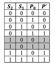
To achieve this desired pumping action a circuit design was constructed around two float switches. A microcontroller was not used for this application to keep the power draw low, as this is a limiting factor given the size of the solar panel that can fit onto the overall system. The logic table required to encode this behavior is shown in adjacent table, where S1 and S2 are the states of switch 1 and 2, respectively, while P0 and P0' are the current and future pump states, respectively. The shaded cells indicate states which should not be possible without a fault
The Equation below describes the output state in terms of the input states and that adheres to behavior outlined in the table above.

Note that the pump state is both an input and an output. The state is therefore separated into two states, P' and P0, to prevent the system from sticking to a single output. A D flip-flop is therefore required transform state P' into P0. This essentially introduces a time step with a period set by a CMOS 555 timer. The resulting simplified block diagram for this pump system can be seen below in the figure.

The actual logic gates will be constructed using NPN transistors instead of gate ICs, as shown in the next figure below. Note the addition of a buffer directly before the relay. Without this buffer, the low resistance pulls the logical output to near ground. While the circuitry provides sufficient current to switch the relay, the low voltage is useless as an indication of pump state P'. The buffer ensures that the pump state is correctly interpreted by the D flip-flop before dropping to provide current for the relay.
